Due to current market conditions, we have suspended online orders.
Due to current market conditions, we have suspended online orders.
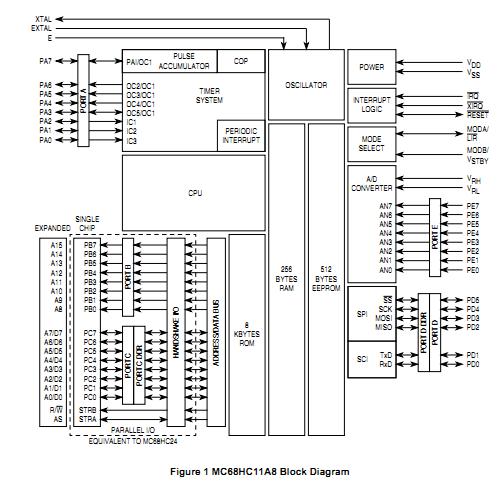
The MC68HC11A1FNR2 is a high-performance microcontroller unit (MCU). The device is based on the M68HC11 Family. The high speed, low power consumption chip MC68HC11A1FNR2 has multiplexed buses and a fully static design. The MC68HC11A1FNR2 can operate at frequencies from 3 MHz to dc.
MC68HC11A1FNR2 absolute maximum ratings: (1)Supply Voltage VDD: –0.3 to + 7.0 V; (2)Input Voltage Vin: -0.3 to + 7.0 V; (3)Operating Temperature Range, TA TL to TH: 0 to + 70℃; (4)Storage Temperature Range Tstg: – 55 to + 150℃; (5)Current Drain per Pin Excluding VDD and VSS, ID: 25 mA.
MC68HC11A1FNR2 features: (1)M68HC11 CPU; (2)Power Saving STOP and WAIT Modes; (3)8 Kbytes ROM; (4)512 Bytes of On-Chip EEPROM ; (5)256 Bytes of On-Chip RAM (All Saved During Standby); (6)16-Bit Timer System: 3 Input Capture Channels; 5 Output Compare Channels; (7)8-Bit Pulse Accumulator; (8)Real-Time Interrupt Circuit; (9)Computer Operating Properly (COP) Watchdog System; (10)Synchronous Serial Peripheral Interface (SPI); (11)Asynchronous Nonreturn to Zero (NRZ) Serial Communications Interface (SCI); (12)8-Channel, 8-Bit Analog-to-Digital (A/D) Converter; (13)38 General-Purpose Input/Output (I/O) Pins: 15 Bidirectional I/O Pins; 11 Input-Only Pins and 12 Output-Only Pins (Eight Output-Only Pins in 48-Pin Package); (14)Available in 48-Pin Dual In-Line Package (DIP) or 52-Pin Plastic Leaded Chip Carrier (PLCC).